Technology.

Optical sensing,
on a chip.

Optics

Optics is a cornerstone technology in sensing applications due to its ability to capture and analyze complex data through the properties of light. The wealth of information carried by light allows for versatile, sensitive detection of a wide range of substances and phenomena in complex samples such as multi-component mixtures or intricate material structures. Its non-invasiveness enables measurements without altering the target. Overall, the precision, non-destructive nature, and data-rich output of optics make it an indispensable tool for advancing sensing capabilities across various industries.

Chip integration

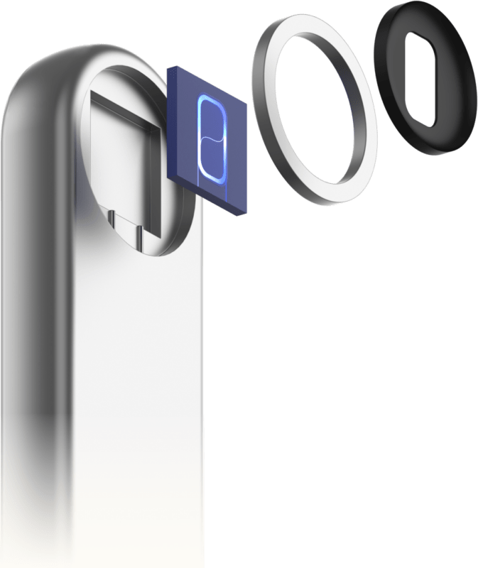
Integrated photonics, or the integration of optical systems on semiconductor chips, builds off the successes of the electronics industry over the last decades. The ability to design and manufacture chips that guide and manipulate light provides optical devices with the same advantages as electronic chips: the miniaturization of complex systems reduces the size, weight, and cost of devices while enhancing their performance. As photonic integrated circuits (PICs) can now be mass-produced with high precision and efficiency, photonic integration has become an indispensable technology with ever-increasing maturity and capabilities.

The benefits of waveguide-enhanced
Raman spectroscopy

Our first sensors rely on Raman spectroscopy, an established analytical method known for being quantitative, highly specific, and compatible with aqueous media. very versatile, as it does not necessarily require previous knowledge of the target species. It is fast and does not require sampling nor sample preparation, making ideally suited to real-time in-line measurements. Waveguide-enhanced Raman spectroscopy (WERS), also called “Raman-on-a-chip”, combines the features of Raman spectroscopy with those of integrated photonics to yield unique advantages for WERS sensors compared to traditional free-space based Raman probes:

Cost

The ability to mass-produce semiconductor chips yields large economies of scale. The integration of components onto the chip also reduces the component count of the system. This results in a sharp diminution in the cost of optical probes.

Size

Nanofabrication allows for the dense integration of optical components on a chip, eliminating the need for bulky, discrete free-space elements. Very long interaction lengths, up to several dozens of centimeters, can be defined on millimeter-sized chips.

Sensitivity

The strong confinement of light in high-index contrast waveguides leads to a concentration of the electric field, that generates enhanced light-matter interactions: a stronger exciting field is delivered to the target molecules, resulting in a stronger Raman response. A larger fraction of the Raman signal is also collected. As this enhanced response is distributed all along the waveguide, WERS is particularly suited to the measurement of bulk solutions.

Speed

Raman spectroscopy doesn’t require sample preparation, is non-destructive and label-free, resulting in measurements directly as the reaction happens. With high sensitivity, only seconds or a few minutes are needed to obtain high-quality data.

Real-time
insights.

Raman spectroscopy is already known for providing in-line, real-time information. Our Raman-on-a-chip sensors go a step further by expanding the range of situations in which Raman can be used: measurements in single-use systems, in small-volume samples, at several points in a reactor or along a line, are now possible. Their reduced footprint allows them to be placed at the exact place where the most relevant information is generated, providing faster response times for dynamic processes.

Our applications.

Bioprocess monitoring

Chemical composition and biological integration in upstream and downstream processes, including in single-use technologies.

Chemical reaction monitoring

Integration in batch and flow chemistry.